
I have been doing more work on flash memories and decided to write up the notes I have been taking.
This article is about the technology behind flash memory: how data is stored, the architecture of flash memories and (briefly) how data is read, written and erased. (This may turn into a series with more detail on various aspects of flash technology.)
Flash cells
The main component of a flash memory cell is a modified field effect transistor (FET). So, first, a brief explanation of how a FET works.
Like any transistor, a FET is an electronic switch that controls the flow of electric current through a channel between two terminals (called the source and drain) by means of a voltage applied to a third terminal, called the gate.

The channel, drain and source are all made from the silicon substrate by the addition of small amounts of dopant elements to control their electrical properties, and hence the type and behaviour of the FET.
When a voltage is applied to the gate, it creates an electric field in the channel which either increases or decreases the conductivity, depending on the type of FET.
A flash memory storage cell is similar to a FET but has an extra, isolated, gate between the control gate and the channel. Charge can be added to, and removed from, this floating gate using quantum tunnelling. A write or program operation involves applying a high voltage to make electrons tunnel to the floating gate. The contents of the cell can be erased by applying a negative voltage to remove electrons from the gate.
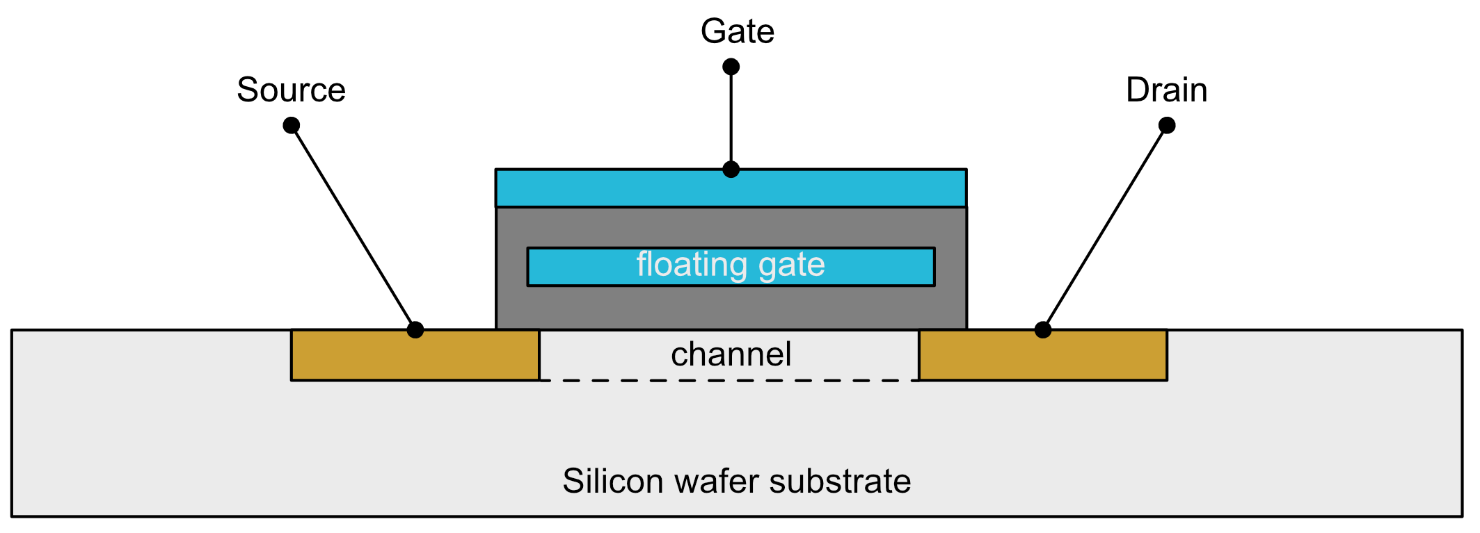
The extra charge on the floating gate changes the how the transistor behaves when a voltage is supplied to the control gate. With no charge on the floating gate, applying voltage above the threshold level (Vt) will turn the transistor on. When a charge is stored on the floating gate, a lower voltage on the control gate will turn the transistor on. A gate voltage between these two levels will only turn on a programmed cell and so can be used to read the data.
Because the transistor pulls the output voltage down to zero when it turns on, a programmed cell represents a data value of 0 while an erased cell represents the value 1.
Flash memory array
Flash memory cells are connected in a hierarchical structure to create the entire memory.
There are two ways of constructing a flash memory array. Multiple cells are connected, either in series or in parallel, to a common bitline that reads or writes the data. These two arrangements are are called NAND and NOR, because of their similarity to the logic gates with those names.

A set of cells connected in series in a NAND structure is called a string. Several strings are used to create an array, with the gates in each row connected to a common wordline, which controls access, to form a page.
Although the NAND structure has some extra transistors, it is still more compact than NOR flash because there are fewer wires (which take up more space than transistors).
An array of pages form a block, which are grouped into a plane. A flash memory chip has one or more planes.

NAND and NOR structures have been targeted at different applications because of their differing characteristics.
Applications
NOR flash is designed to be used as a replacement for earlier types of erasable and programmable read-only memory (EPROM or EEPROM). As such, it is optimised for random access reads and writes. However, because it is intended to be read more often than written, write speeds are about 100 times slower than reads. NOR flash is available with a standard parallel memory interface (address, data and control signals) or a serial interface such as SPI. Serial NOR flash devices can be smaller, lower power and lower cost.
When used for code storage, the slower speed of serial flash means that it may be necessary to copy the code to RAM before executing it. Faster SPI implementations can be used with a microcontroller that maps the serial interface into the processors memory space so that code can still be executed “in place”, i.e. directly from the serial flash.
NAND flash is optimised for high density storage so it is used in applications such as SD cards and solid state drives (SSDs). To further improve density, NAND memory removes much of the address decoding logic which is not required in its applications, where data is read sequentially. It is also designed to provide similar read and write speeds, as required by mass storage applications.
Summary
| NAND | NOR | |
| Read speed | 30 MB/s | 30 – 60 MB/s |
| Write speed | 8 MB/s | 0.2 – 0.5 MB/s |
| Erase speed | Fast (3 ms) | Slow (1 – 5 s) |
| Access | Sequential / block | Random |
| Interface | IO mapped | Memory mapped or serial |
| Applications | Mass storage / SSD | ROM / non-volatile RAM |